
-
TRANSDUCERS
- TRANSDUCERS
-
BASIC COMPONENTS DK
- BASIC COMPONENTS DK
-
MARKETPLACE
- MARKETPLACE
-
DEVELOPMENT BOARDS & KITS
- DEVELOPMENT BOARDS & KITS
-
CABLE ASSEMBLIES
- CABLE ASSEMBLIES
-
RF AND WIRELESS
- RF AND WIRELESS
-
BOXES ENCLOSURES RACKS
- BOXES ENCLOSURES RACKS
-
AUDIO PRODUCTS
- AUDIO PRODUCTS
-
ARTILA
- ARTILA
-
FANS-BLOWERS-THERMAL MANAGEMENT
- FANS-BLOWERS-THERMAL MANAGEMENT
-
WIRELESS MODULES
- WIRELESS MODULES
-
TERMINALS
- TERMINALS
-
Cables/Wires
- Cables/Wires
-
SINGLE BOARD COMPUTER
- SINGLE BOARD COMPUTER
-
BREAKOUT BOARDS
- BREAKOUT BOARDS
-
LED
- LED
-
TEST AND MEASUREMENT
- TEST AND MEASUREMENT
-
POTENTIONMETERS AND VARIABLE RESISTORS
- POTENTIONMETERS AND VARIABLE RESISTORS
-
DEVELOPMENT BOARDS AND IC's
- DEVELOPMENT BOARDS AND IC's
-
EMBEDDED COMPUTERS
- EMBEDDED COMPUTERS
-
OPTOELECTRONICS
- OPTOELECTRONICS
-
INDUSTRAL AUTOMATION AND CONTROL
- INDUSTRAL AUTOMATION AND CONTROL
-
COMPUTER EQUIPMENT
- COMPUTER EQUIPMENT
-
CONNECTORS & INTERCONNECTS
- CONNECTORS & INTERCONNECTS
-
MAKER/DIY EDUCATIONAL
- MAKER/DIY EDUCATIONAL
-
TOOLS
- TOOLS
-
MOTORS/ACTUATORS/SOLEENOIDS/DRIVERS
- MOTORS/ACTUATORS/SOLEENOIDS/DRIVERS
-
FPGA HARDWARE
- FPGA HARDWARE
-
POWER SUPPLIES
- POWER SUPPLIES
-
ROBOTICS & AUTOMATION
- ROBOTICS & AUTOMATION

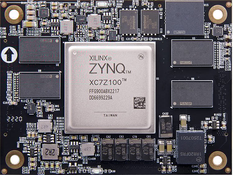
ARM+FPGA SOC technology
2x ARM Cortex-A9, Industrial grade
Product parameters
Core Board Parameters
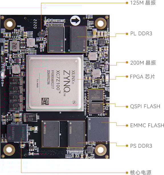
Core board-AC7Z100B
FPGA Chip-XC7Z100-2FFG900I
Chip CPU-2x ARM Cortex-A9, Dominant frequency 800MHz
PL RAM-1GB DDR3, Data rate 1600Mbps
PS RAM-1GB DDR3, Data rate 1066Mbps
Speed Grades- -2
Chip Level-Industrial grade
Working Temperature--40°C~85°C
Logic Cells-444K
Lookup table-277400
trigger-554800
Multiplier-2020
transceiver-16 -Channels, supporting PCIe Gen2 x8
Block RAM-25.6Mbit
MIO-37
PL IO-162
Adjustable voltage IO-96
LVDS differential pair-48
Functions and interfaces
EMMC FLASH-8GB EMMC flash chip is used to start the storage configuration and system files
QSPI Flash-Two 256Mbit QSPI flash for FPGA user data storage
AD converter-ADC is integrated inside the chip, 2 AD converters, which can measure on-chip voltage and temperature sensing, 17 external differential input channels, and the sampling rate is 1Mbps
Crystal oscillator-One crystal oscillator 33.333mhz provides clock input for PS terminal. A differential crystal oscillator 200MHz is used as the clock source of PL system and the reference clock of DDR3 controller. A differential crystal oscillator 125MHz provides a reference clock for GTX transceiver
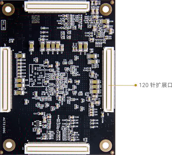
Expansion port-Four 120 pin Panasonic industrial grade connectors
Power parameters
input voltage-5V power supply
Packing list
FPGA core board-1
FPGA core board-1
structure size
Size-80mm x 60mm x 10.8mm
Connector closing height-3.0mm
Number of laminations-12 layer PCB board design
- Home
- XILINX FPGA
- Xilinx ZYNQ7000 SoC ARM SOM FPGA Core Board XC7Z100


Xilinx ZYNQ7000 SoC ARM SOM FPGA Core Board XC7Z100
SIZE GUIDE
Your enquiry has been sent
Product Enquiry Form
Leave us a message for futher information.
- Lead time is 3-4 weeks
Description of product
ARM+FPGA SOC technology
2x ARM Cortex-A9, Industrial grade
Product parameters
Core Board Parameters
Core board-AC7Z100B
FPGA Chip-XC7Z100-2FFG900I
Chip CPU-2x ARM Cortex-A9, Dominant frequency 800MHz
PL RAM-1GB DDR3, Data rate 1600Mbps
PS RAM-1GB DDR3, Data rate 1066Mbps
Speed Grades- -2
Chip Level-Industrial grade
Working Temperature--40°C~85°C
Logic Cells-444K
Lookup table-277400
trigger-554800
Multiplier-2020
transceiver-16 -Channels, supporting PCIe Gen2 x8
Block RAM-25.6Mbit
MIO-37
PL IO-162
Adjustable voltage IO-96
LVDS differential pair-48
Functions and interfaces
EMMC FLASH-8GB EMMC flash chip is used to start the storage configuration and system files
QSPI Flash-Two 256Mbit QSPI flash for FPGA user data storage
AD converter-ADC is integrated inside the chip, 2 AD converters, which can measure on-chip voltage and temperature sensing, 17 external differential input channels, and the sampling rate is 1Mbps
Crystal oscillator-One crystal oscillator 33.333mhz provides clock input for PS terminal. A differential crystal oscillator 200MHz is used as the clock source of PL system and the reference clock of DDR3 controller. A differential crystal oscillator 125MHz provides a reference clock for GTX transceiver
Expansion port-Four 120 pin Panasonic industrial grade connectors
Power parameters
input voltage-5V power supply
Packing list
FPGA core board-1
FPGA core board-1
structure size
Size-80mm x 60mm x 10.8mm
Connector closing height-3.0mm
Number of laminations-12 layer PCB board design
Related products


NEWSLETTER
Subscribe to get Email Updates!
Thanks for subscribe.
Your response has been recorded.
INFORMATION
ACCOUNT
ADDRESS
Tenet Technetronics# 2514/U, 7th 'A' Main Road, Opp. to BBMP Swimming Pool, Hampinagar, Vijayanagar 2nd Stage.
Bangalore
Karnataka - 560104
IN
Tenet Technetronics focuses on “Simplifying Technology for Life” and has been striving to deliver the same from the day of its inception since 2007. Founded by young set of graduates with guidance from ardent professionals and academicians the company focuses on delivering high quality products to its customers at the right cost considering the support and lifelong engagement with customers. “We don’t believe in a sell and forget model “and concentrate and building relationships with customers that accelerates, enhances as well as provides excellence in their next exciting project.