


XILINX Zynq-7000 SoC SoM FPGA Core Board XC7Z020
- Lead time is 3-4 weeks
- Call for pricing
Description of product
ARM+FPGA SOC Technology
Ultra Small Size, Dual-Core ARM Cortex-A9, Industrial Grade
PRODUCT PARAMETERS
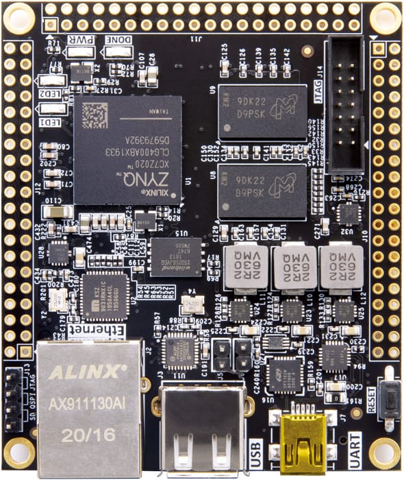
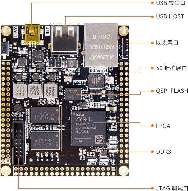
Core Board Parameters
Core Board Chip-AC7020
FPGA Chip-XA7Z020-1CLG400I / XC7Z020-2CLG400I
Kernel-Dual-Core ARM Cortex-A9
RAM-DDR3 1GB, Data Rate 1066Mbps
Chip level-Industrial grade, working temperature -40 °c~85 °C
Logic Cells-85K
Look-Up Tables ( LUTs )-53,200
CLB Flip-Flops-106,400
Multiplier-220
Block RAM-4.9Mb
PS MIO-8
PL IO-94
Interface and Function
DDR3-Can be Used as ZYNQ Chip Data Cache, Operating System Memory
QSPI Flash-256Mbit, Used for Storage of System Files and User Data
Crystal Oscillator-33.333Mhz, Provide Stable Clock Source for the PS System,50MHz, Provide Extra Clock for PL Logic
Gigabit Ethernet-10 / 100 / 1000M Ethernet with RJ-45 Interfaces for Data Exchange
JTAG-14-Pin JTAG Interface to Debug and Download ZYNQ System
LEDs-2 User LEDs, 1 Controlled by PS, 1 Controlled by PL
USB HOST-Used for Connect USB Peripherals such as Mouse, Keyboard and U-Disk
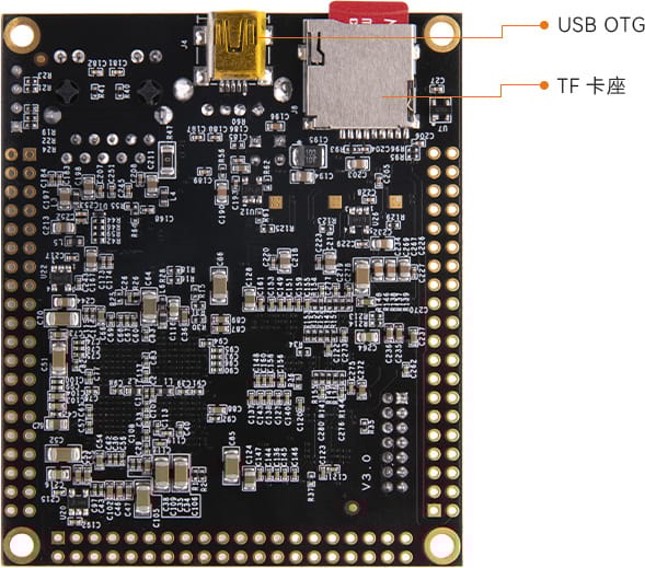
USB OTG-Used for OTG Communication with PC or USB Device
USB Uart-Used for Power the board or Serial Communication with External Devices
KEYs-1 Reset Keys, used to reset CUP
Expansion Port-Three 40-Pin Expansion Ports (0.1 inch Pitch), Expand the IOs Connect with 7 inch LCD Screen, Camera, AD / DA and Other Modules.
Micro SD Card Slot-1 Micro SD TF Card, Store Operating System Image and File System
Start Mode-Three Startup Modes: JTAG Debugging, QSPI FLASH and SD Card
Power Supply Parameters
Power by-USB Cable
Package List
FPGA Core Board-1
Card Reader-1
Mini USB Cable-1
Pin-2
TF Card-1
Pillar-4 Pieces
Structure Size
Size Dimension-2.95 inch x 2.52 inch
Number of Layers-8-Layer FPGA Development Board PCB


